September 2025
From: Brian, Tobias, and Gaby
Subject: Incumbent Weaknesses?
Welcome back to the BT&G Infrastructure Newsletter. We hope this finds you well with fall in full swing.
The story is out: semiconductors rule the world. The mind-bending, jaw-dropping, WTF-is-going-on-here deals keep coming. In this month, we’ve seen:
- $100B investment in OpenAI from Nvidia a deal to acquire 10 GW of Nvidia capacity
- AMD agreeing to supply 6 GW of compute capacity to OpenAI in exchange for OpenAI investment in AMD (up to 10% equity!)
- OpenAI and Oracle signing a $300B cloud deal
- xAI raising $20B, with $2B supposedly coming from Nvidia
- On the accelerator front: Cerebras raised $1.1B, Groq raised $750M, Rebellions raised $250M, and Upscale raised $100M
- OpenAI and Broadcom partnering on 10GW of custom AI chips designed by OpenAI
AI is buoying the US economy, circular revenue is trending, bubble talk is bubbling, and visuals like these abound:
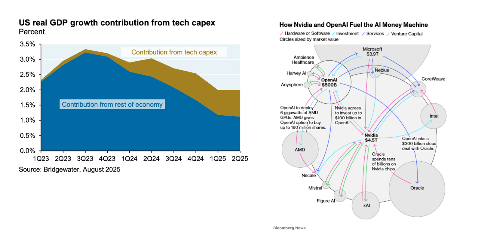
Two things are obvious to us: astronomical value creation and epic trainwrecks are on the horizon. The tech sector is investing at historic scale, with compute capex now at 1.2% of GDP – yet this pales against truly transformative infrastructure buildouts like the 1880s railroad boom, which peaked at 6% of GDP. If the industry is right that we're laying the physical foundation for machine intelligence, we may have barely begun. The investment cycle could expand five-fold from here.
Obviously we’re not the only AI bulls here, nor is our compute interest unique. But despite all the public attention on NVIDIA, the massive capex outlays, power shortages, and more, the semiconductor industry is overlooked at seed. In 2024, semiconductor startups raised roughly $275M in seed capital, just a fraction of the $30B global seed market. The disparity is understandable: practically zero exits in semis over the last two decades, while many VCs lost their shirts trying; the category is extremely technical, painfully capital-intensive, and the incumbents are dauntingly powerful. But in our experience with backing companies like Etched, Atero (now a part of Crusoe), and several unannounced investments, we know that startups will play a prominent role in the next era of compute.
The GPU – extraordinarily powerful, capable of billions of operations per second – sits at the heart of the AI revolution. But everything around it is struggling to keep up. Models scaled from a few billion parameters to 5-10T with GPT-5. Context lengths have grown from 4K in the initial ChatGPT product to 400K in GPT-5-Pro. Reasoning uses 20x more tokens at inference-time. All of this requires more memory and, in turn, more power, networking and custom servers. The surrounding systems to the GPU are overwhelmed.
Is the semiconductor industry up to the task? The sector is run by powerful duopolies and oligopolies, but they are exposed to systemic weaknesses. They are structurally tied to long R&D time; they’ve invested relentlessly in supply chain optimizations for a select set of products; their powers lie in both scale and deeply entrenched relationships with fabs and customers. Radical changes will cannibalize existing business lines and new talent is emerging focused on big swings.
This newsletter examines four areas with daunting incumbents and real opportunities for startups. The table below breaks down categories in the semiconductor value chain that we’ll cover today, illustrating the scale of each market.
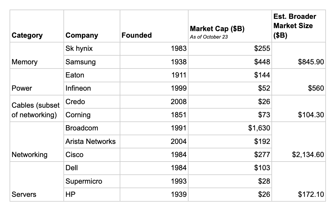
Memory
Memory is the second most valuable segment of the semiconductor value chain after GPUs, raking in $170B in revenue in 2024. Memory’s importance is driven by the steep increase in model sizes, which are stored in memory, and memory-intense architectures like reasoning models, that are becoming the default. Memory bandwidth and speed of data access is slowing workloads, not the GPU’s compute capabilities, resulting in the “memory wall”. Hence, memory has emerged as a key bottleneck to AI’s growth.
High bandwidth memory (HBM), which SK hynix first debuted in 2013, is the defacto memory solution for AI accelerators. SK hynix controls over 62% of the HBM market, ahead of Micron (the only American memory company) at ~21% and Samsung at 17%. HBM has boosted the value of companies like SK hynix (up almost 20% in the past five days!) that can meet demand.
HBM is built by stacking memory (specifically DRAM) chips vertically and linking them with ultra-fast connections, delivering far more data per second than alternatives and powering most of today’s AI accelerators. It packs a ton of data in a small space, and places that data very close to the GPU, but off-chip unlike SRAM or caching that happens on-chip, for fast access. The blue rectangles below represent a single stack of HBM, made up of 4 DRAM chips.
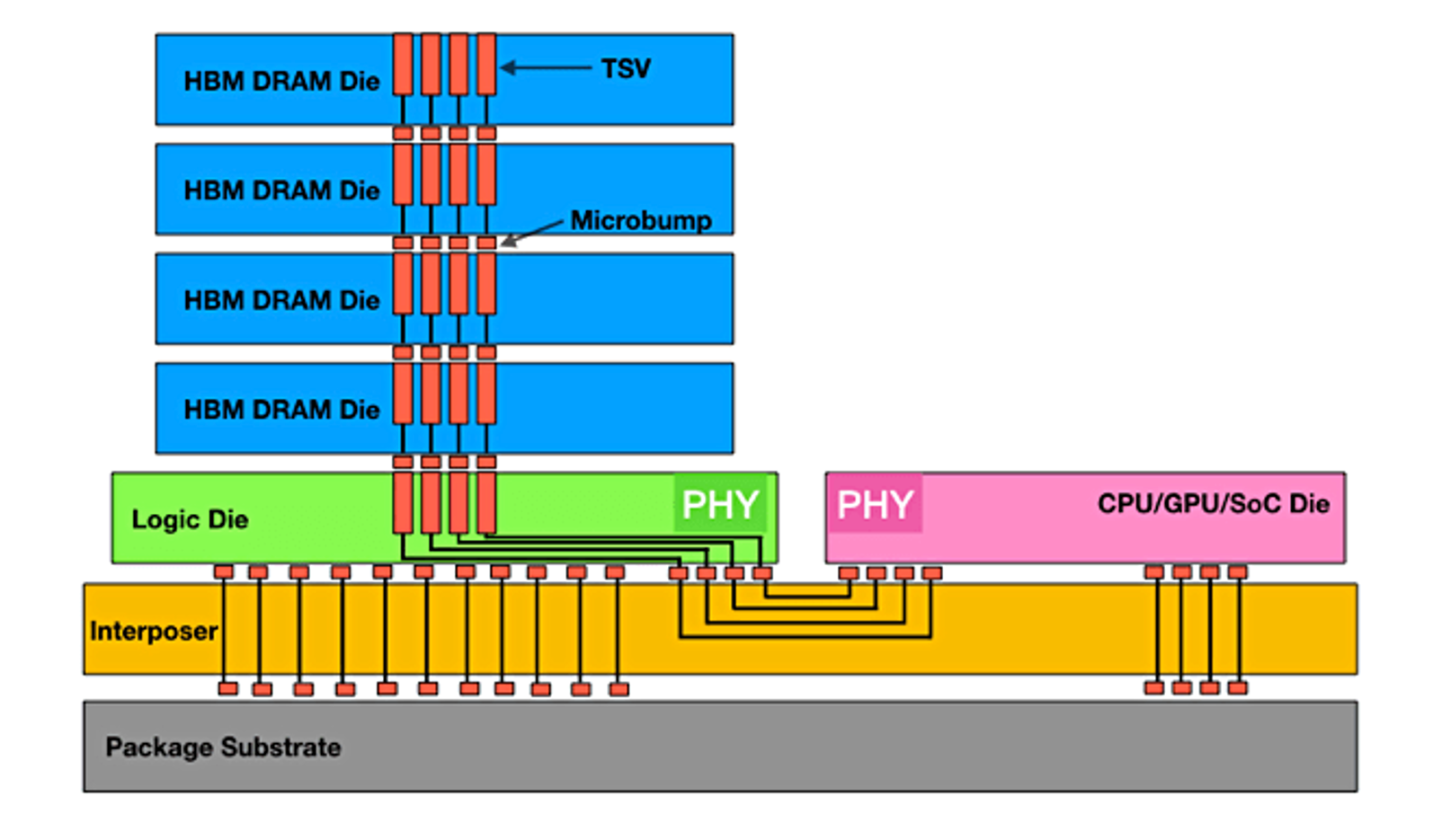
On an Nvidia B200, there is 192 GB of HBM (8 stacks around a GPU, like 8 of the visual above), compared to 80GB on its predecessor, the H100. A 70B-parameter model, tiny by today’s standards, needs ~140 GB for weights alone, which is ~2x the HBM capacity on an H100. The need for more memory capacity is clear as day – Nvidia plans to have 1TB of memory per package (4 GPUs) at the Rubin Ultra.
HBM is expensive, compared to standard server memory, for a few reasons – the manufacturing complexity of stacking DRAM results in lower yield, only a handful of foundries can package HBM, and it is supply constrained by 3 players with a ton of pricing power. As a result, HBM accounts for ~30-40% of BOM per GPU.
The incumbent’s R&D investments are massive – Sk hynix spent $2.5B in a single quarter last year. They have deep IP portfolios (Sk hynix has a portfolio of over 100k patents). Unlike chip design companies, memory companies own and operate their fabs. This vertical integration means they heavily invest in manufacturing optimizations, alongside R&D efforts to manage rising heat and power constraints, with roadmaps being driven by the needs of their chip company customers. Their R&D timelines are incredibly long – Sk hynix shared a 30 year DRAM roadmap earlier this year. Beyond R&D, they benefit tremendously from scale. This is what makes them formidable opponents.
Yet, we see three opportunities for startups.
First – ride the HBM wave! Two ideas here are thermal management and manufacturing optimization. For HBM3 (used in H100s), Sk hynix’s yield is only 60-70%, compared to over 90% for regular DRAM. Startups that reduce defect rates, even just a small percentage, can unlock a huge revenue opportunity. Sk hynix sold $5B in HBM in Q2 2025 and are shipping 170k HBM wafers this year (~$115k per wafer). Let’s assume that was 65% yield, meaning they made 261k units, losing 91k units to yield. If Sk hynix was able to improve to just 66% yield (about 2,600 more wafers), they’d unlock $300M in new revenue.
Thermal optimization is another opportunity to ride the HBM wave – the stacked structure of HBM traps more heat than alternative memory approaches. 30% of a package’s power goes to powering memory. Memory stacks are more sensitive to heat than a GPU is. Underfill is a material commonly used to improve heat dissipation around memory blocks, as well as through-silicon vias (TSVs) which move heat away from HBM stacks. Finding alternatives that improve heat dissipation and let HBM stacks work at full capacity is an opportunity for new companies.
Second – reduce reliance on HBM. One approach is memory pooling, where many compute resources share access to a common pool of remote memory, limiting HBM usage to a smaller subset of low-latency, heavily-accessed local data. There are compelling approaches here like what RAAAM is building, a powerful SRAM replacement that reduces the strain on HBM. Or, pick existing memory alternatives. This is the approach Groq is taking. They use no HBM on their chips. It’s a hedge against the supply constraints on the market They have a single, monolithic, on-chip SRAM memory system versus HBM, prioritizing latency that can come from an on-chip system versus an off-chip HBM system. The tradeoff, however, is that on-chip has far less capacity, which can dramatically limit the size of a model that can be stored on the device. It would take ~4K Groq LPUs to serve Deepseek’s 671B parameter model. Furthermore, yields for SRAM-heavy chip designs are lower than those of standard GPUs/AI accelerators, reducing the cost advantage.
Last – evolve beyond today’s HBM and build memory solutions for the next decade. We’re seeing new, in-memory compute (Samsung has prototyped AI engines inside HBM banks, pushing what’s possible here), ferroelectric RAM (by Sunrise and FMC), to name a few.
Net new approaches pose promise in the memory market. HBM, despite being the best in class solution for most chips today, is a clunky, complex solution to memory bandwidth and storage. There are innovative ideas out there that will fundamentally reimagine HBM, pushing memory to be an enabler, not a bottleneck, to GPU efficiency.
Power Electronics
Power, from generation to delivery, is the constraint de jure on the multi-trillion dollar infrastructure buildout. Contracts are now being reported in watts, like OpenAI acquiring 26GW (think all of Switzerland's electricity capacity!) across Broadcom, Nvidia, and AMD. Power generation is a slow, regulated industry that can’t match the pace for AI (hence why Elon bought an overseas power plant for Colossus). While generation struggles, efficiency has become paramount.
A decade ago, one data center rack consumed less than 10kW. Today, an AI rack can draw upward of 100kW, with forecasts of 600kW by 2027 (think 500 U.S. homes!). From generation to GPU, there are ~10 steps of power conversion, with power loss occurring at each step as a result of physics and poorly optimized power electronics. For a 100kW rack, you’ll need to generate roughly 300kW of power to account for losses. The scale of losses means even single-digit efficiency gains are worth billions, driving up tokens per watt, a key KPI behind the “tokenomics” that hold up the AI economy.
The power electronics market is over $40B, made up of converters, power distribution systems, regulators, and more, controlled mainly by Infineon, Eaton, and Texas Instruments. Power electronics is horizontal across automotive, consumer electronics, and energy, with data centers being the fastest growing customer segment of the past few years.
Most incumbent power electronics rely on silicon – a mature, cheap, and well-understood material. As AI systems scale to unprecedented power levels, silicon is hitting its physical limits – it wasn’t designed for this magnitude of demand. Silicon carbide (SiC) and gallium nitride (GaN) have emerged as materials that offer much needed improvements, including greater thermal tolerance and improved conductivity. These materials can theoretically cut energy loss by 50% or more compared to silicon and double power density. The incumbent dominance – built on decades of optimization around silicon, legacy packaging, and a focus on buyers in consumer electronics or automotive – is presenting as a weakness as markets push to new materials.
Opportunities in power electronics span three fronts: making new material manufacturing more efficient, building data center-optimized products, and leapfrogging today’s limits through new material discovery.
As for manufacturing – SiC wafers are difficult to manufacture at scale. Growing SiC crystals, of which wafers are sliced from, requires more energy due to higher heat (2,000 degrees Celsius vs. 1,425 for silicon) and more time (100-300x slower to grow SiC vs. silicon) required. Gallium nitride is often grown on a silicon substrate, which yields complexity when working across two materials that results in defects. Given low yield, the cost per device remains multiples higher than traditional silicon electronics. Innovations on manufacturing that directly impact the conditions needed for these new materials present an opportunity for startups.
As for the data center customer – for decades, incumbents have served predictable, slow-moving end markets across automotive, industrial, and consumer electronics. 60% of Infineon’s sales are to automotive buyers. Their fabs, product roadmaps, and qualification processes were never built for AI market demands, despite working hard to keep up. Eaton alone saw data center sales grow 45% year over year. New entrants to the power electronics space have the potential to meet the newest, neediest customer with the speed, flexibility, and efficiency they demand.
The last opportunity is in new material discovery. Silicon carbide and gallium nitride have a ways to go for mainstream adoption. However, AI-enabled materials discovery processes may yield a material that is higher conductivity, has better thermal management, and lacks the complexity of manufacturing that SiC and GaN do today. Startups with deep research experience are poised to create leapfrog technology here.
AI has forced our hand on power. Solutions of the cloud-era aren’t sufficient for the exploding power demands of an AI-era. Incumbents are poorly positioned to capitalize on the newest technology needed for the power-hungry systems being deployed today.
Networking
Networking spans cables, switches, routers, interconnects, and the software that moves data between and within racks. As AI demand and model sizes grow, GPU clusters like xAI’s Colossus are scaling from 100K to 1M GPUs. This massive footprint strains existing networking, especially latency.
Cables, a $15B slice of the $100B+ networking market, carry data as electrical or optical signals between chips, servers, and racks. Copper dominated early telecom for its conductivity, durability, and cost. But as data centers scaled in the 2000s, fiber optics, pioneered by Corning, took over long-reach connections. Corning remains a critical supplier to Nvidia, and its stock has doubled in six months amid the optical buildout.
In an AI era, short-reach (intra-rack) copper cables are fragile. Copper is reaching its physical limits – signal loss, heat buildup, and sheer weight – in a response to growing bandwidth and power demands. Modern AI switches using copper now push 224 Gb/s per lane, but whether it can scale to 448 Gb/s remains uncertain. But scaling down optics from long-reach has proven to be a physics challenge given signals are sensitive at short distances, resulting in signal loss and noise in data transfer. Corning isn’t well positioned to cannibalize their existing product line by moving beyond optics.
We see two opportunities within cables.
First, crack the challenge that is short-range optics. That’s where startups like Ayar Labs, Celestial AI, and Lightmatter are making a compelling push to prove out intra-rack photonics as a feasible alternative to copper. Ayar Labs claims 10x lower latency and ~6x better power efficiency than optics that are in the market today.
Second, move beyond optics. Outside of photonics, dielectric cables present a leapfrog technology that optics incumbents aren’t well positioned to move into – different materials, analog components, digital control components, supply chains and more. Unlike optical cables, which transmit light through glass fibers, dielectric cables, like Point2, guide high-frequency electrical signals through plastic waveguides. As a result, Point2’s dielectric cables can 10x the reach of copper cables, while using 3x less power than its optical counterparts.
There exist several networking opportunities beyond cables. When Mellanox was acquired, it was a great move for Nvidia, but also closed off a lot of the market. We are encouraged by open ecosystems, such as Ultra Ethernet and UALink, being promoted by companies like AMD, Broadcom, and Meta. There is significant innovation in the design of network-interface-cards, both expanding their AI capabilities and packaging them closer to the GPUs for lower latency. Additionally, there’s potential for an open-source ecosystem to take on Infiniband, or software to improve dynamic routing of workloads to highly optimized hardware.
Networking remains a massive prize and it matters now more than ever as we push the limits of intra- and inter-rack data movement.
Servers
Servers are the backbone of the internet and AI. We define a server as the physical containers that contain the GPU, CPU, memory and surrounding components including power and networking, that live in a rack within a data center. Servers in the cloud era were built for predictable, CPU bound workloads, and have not evolved to meet the needs of the AI era, Modern accelerators draw kilowatts of power, generate extreme heat, need to store and access massive amounts of data and depend on ultra-low-latency connectivity, that fundamentally differs from the demands of a cloud computing era.
Currently, Dell owns ~20% of the server market, followed closely by HP, Inspur, and Lenovo. The incumbent approach has been to optimize for scale, offering standardized server offerings that lack flexibility for customization. Supermicro’s surge is proof of an opening for flexible server offerings: by moving faster to integrate NVIDIA and AMD’s newest chips, Supermicro has captured a disproportionate share of AI demand (70% of revenue now tied to GPU systems). Dell is also a formidable (and growing) player here. They ended their latest quarter with a $14B backlog in AI-optimized server orders.
That’s just the OEM story. The landscape is much more complex – configuration is decided by the OEMs (Dell, HP, Lenovo) or the hyperscalers or the chip companies (Nvidia, AMD). Flexibility is king, as everybody is squeezing efficiency out everywhere.
The hyperscalers want more autonomy. As a result, we’ve seen a growth in the use of ODMs (Foxconn, Quanta) – original device manufacturers. Amazon partners with Quanta, a Taiwanese ODM, to build hardware aligned to their bespoke specs, at a better price than the OEMs. Even with this customization, the ODMs are not highly innovative in their offerings – they manufacture in countries with cheap labor, using commodity products. The ODM model is under pressure, as margins are tight. Foxconn is a ~6% gross margin business.
The rise of the ODM indicates that there is an opportunity for startups. We’ve seen a driving force through the Open Compute Project (OCP) encouraging open innovation in the infra stack. As more hyperscalers use ODMs versus locked-in OEMs, there is more incentive for component level innovation. It also means that hyperscaler buy-in is king in order to scale adoption of innovations at a power electronic, CPU, or memory level.
We see two opportunities in servers, across design and IP.
Given the increased customization of server deployments, a new startup could operate as a co-designer, integrating all the latest technology into a more flexible server offering. From an IP perspective, a next-gen ARM for server design could respond to increasing complexity coming to servers through photonics, in-chip cooling, and new power delivery methods.
The server market is shifting from standardized, mass-produced systems to highly customized architectures purpose-built for AI. As hyperscalers demand greater control over design and performance, the lines between OEMs and ODMs are blurring – creating an opening for startups to innovate across hardware, software, and IP.
The road ahead
AI’s infrastructure buildout is exposing deep cracks in the semiconductor value chain – and with them, rare moments of opportunity. Across memory, power, networking, and servers, the incumbents are constrained by scale, legacy design choices, and a hesitancy to disrupt their own cash cows. The next generation of compute will be won by those willing to rebuild the stack around AI’s extreme demands for power, bandwidth, and flexibility.
The semiconductor industry continues its steady, incremental march – sophisticated, but slow. This has worked, historically, but AI’s demand is intensifying the need for compute more than ever in history. Step function improvements will come from new teams taking bold risks to build for the AI world.
We’re believers that young founders partnering with experienced teams from these industries are going to be how new entrants win. Pairing fresh perspectives and visionary ambition with deep technical experience is a founding team we’re excited to meet.
We’d be remiss not to mention that our compute team at Primary has grown. We’ve welcomed Jason Lango as an Incubation Venture Partner and Ross Pantone as an Operator-in-Residence focused on semiconductors, marking our first hires as a firm in the Bay Area. We’re lucky to have them as collaborators on this newsletter and on everything we’re building and backing in compute.
As always, if you have any thoughts, feedback, or know someone we should meet, let us know!
Best,
Brian, Tobias and Gaby